Summary of LPDDR6

LPDDR6 (Low Power Double Data Rate 6) is the next-generation low-power memory standard for smartphones, tablets, thin laptops, on-device AI, and automotive systems. JEDEC published it in 2025 as JESD209-6. Compared with LPDDR5 and LPDDR5X, it is faster and more efficient: typical speeds start around 10,667 MT/s and can reach 14,400 MT/s, giving each chip roughly twice the bandwidth of LPDDR5X. It does this with a wider, split-channel design that can serve more requests at once while still fetching small chunks of data when that is all the system needs.
LPDDR6 also uses lower core voltages and smarter power modes, including the ability to idle half the interface when demand is light. Vendors generally claim about 20–30% better energy efficiency than LPDDR5X. Reliability is stronger too: on-chip error correction is required, and the standard adds protections against data corruption and reserved areas for critical information.
Interposers for Interfacing Test Equipment to the LPDDR6 Bus
Validating an LPDDR6 interface is more demanding than LPDDR5/LPDDR5X. JESD209-6 devices run at 10,667–14,400 MT/s on a 24-bit channel split into two independent 12-bit sub-channels, each with its own compact CA bus, lower dual-rail VDD2 supplies (nominally ~1.0 V / ~0.875 V), and 0.5 V I/O that can scale lower under DVFS. Eye openings are small, timing budgets are tight, and interposer designs that are acceptable on earlier LPDDR generations can close the eye or disturb training. Xcelerate™ series interposers for LPDDR6 provide a controlled probe point at the DRAM BGA so an oscilloscope, logic/memory analyzer, or protocol analyzer can observe DQ, CA, CK/WCK, and related strobes with minimal loading.
Attachment Service
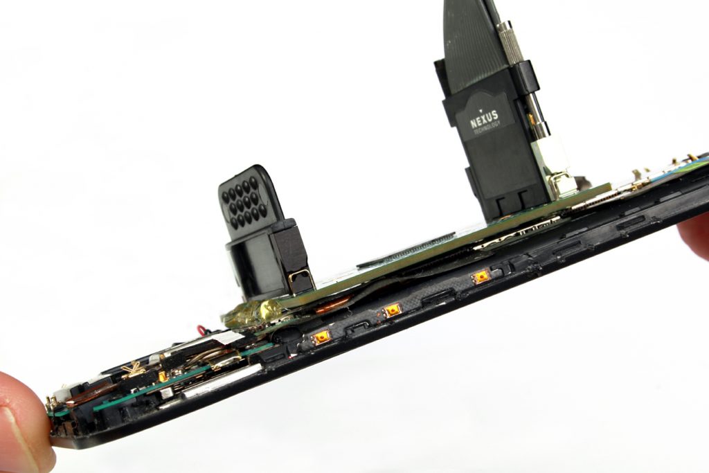
Nexus Technology’s expert attachment service provides a ready-to-go test solution customized to your application. We will attach the interposer and any additional accessories to your application’s target. We can also power-on and test your application to confirm functionality.